This is the first article in a series that I call ‘Learning Electronics’. The goal is to learn and experiment with basic electronic circuits. The first circuit I will discuss here is the astable multivibrator. This is a very simple oscillator circuit that can be used to generate square waves. Here is the schematic of a standard astable multivibrator:
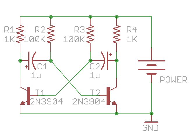
It consists of only two NPN transistors (T1 and T2), two capacitors (C1 and C2), and four resistors (R1-R4), organized in a symmetric fashion. The collectors of T1 and T2 are outputs, which provide complement square wave signals. The values of the capacitors and resistors can vary depend on the desired frequency, and their values do not have to be symmetric.
Update: as some readers pointed out, for square wave output, the resistor values should satisfy: R2 / R1 < h_fe, where h_fe is the transistor's current gain (same for R3 and R4). As h_fe is usually around 80 to 250 for 2N3904, the specific values above (R1=1K, R2=100K) are close to the margin. To improve this, consider increasing R1 or decreasing R2. Alternatively, you can replace 2N3904 with BC547, or even a Darlington transistor (e.g. MPSA14), which have higher h_fe values.
Principles
So how does the circuit work? To begin, when power is applied, theoretically both T1 and T2 should turn on, since their base pins are connected through resistors (R2 and R3) to Vcc. However, due to small differences in the electric properties, one of the them will turn on slightly earlier than the other. Without loss of generality, let’s assume T2 turns on first. Therefore, T2’s collector begins to conduct and can be thought of as ‘shorted’ to ground. Note that C2’s right lead is connected to T2’s collector, and since C2 is not charged yet, its left lead also has a voltage close to ground. This immediately shuts off T1, i.e. T1 becomes an open circuit. Therefore C1’s left lead is in floating status, and its right lead is connected to T2’s base, which is about 0.7V due to the forward voltage drop of transistors. This forward voltage drop is the same as a diode. So at this moment, the circuit is equivalent to the following:
During this period, T2’s collector (output O2) remains low, and C2 begins to charge through R3. Thus the voltage on C2’s left lead will rise, and the rising time depends on R3 x C2. At the same time, C1 also charges, through R1, which is typically a small resistor (e.g. 100-1000 ohm). So C1’s left lead (output O1) will quickly rise up to Vcc and remains high.
As C2 continues to charge, a critical moment will happen when its left lead rise up to 0.7V, at which moment transistor T1 will turn on, and its collector will conduct to ground. Note that since C1’s left lead is connected to T1’s collector, it will also drop to ground voltage. As C1 is fully charged, it’s right lead will suddenly drop to a negative voltage (-Vcc). This will shuts off T2 firmly. Therefore the circuit will suddenly transition to the following equivalent:
During this period, output O1 will remain low, and output O2 will quickly rise to Vcc (due to the charging of C2 through a small resistor R4). At the same time, C1 charges through R2 and the voltage on its right lead will rise over time determined by R2 x C1. Now you can predict what’s going to happen: as C1 continues to charge, the next critical moment happens when C1’s right lead rises above 0.7V. At that point, T2 will conduct again while T1 shuts off. The same cycle will repeat. There you go, oscillators!
Analysis
Now we have to do some calculus to find out the frequency of the oscillator. Let me focus on output O2. As it alternates between low and high, it approximates a square wave. How to find out the frequency? Note at the end of stage 1, C1 has a voltage of (Vcc – Vb) across it (where Vb = 0.7V). Again, the voltage establishes very quickly because R1 is small. The moment the circuit transitions from stage 1 to stage 2, C1’s right lead has an initial negative voltage: -(Vcc – Vb), and the circuit remains in this stage until that lead rises up to +Vb. So let’s calculate how long this will take. There are ready-made equations to compute this, but here let me derive it from basic differential equations.
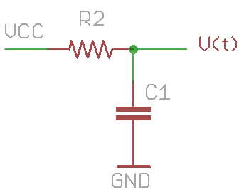 To start, the problem can be simply stated as follows: a resistor R2 and capacitor C1 are connected in series between Vcc and ground. C1 has an initial voltage of -(Vcc – Vb). How long does it take for C1’s voltage to rise up to +Vb? Let’s assume C1’s voltage is V(t): a function that changes over time. According to the law of capacitor, the change of V(t) is equal to the current flowing through it divided by the capacitance:
How much is the current i(t)? That’s equal to the current flowing through the resistor R2, thus
putting them together:
This is a simple differential equation. We can rearrange it to the following form:
By using the fact that
and integrate both sides, we get:
where K is a constant. Using the knowledge that when t=0, V(t)= -(Vcc – Vb), we find out
so:
Recall that our goal is to find hen V(t) is equal to Vb, so substitute Vb to V(t), and solve for t:
Under the assumption that Vcc is much larger than Vb, this is approximately equal to:
This is how long stage 2 will last. Similarly, stage 1 will last for approximately
Therefore, a full cycle will take
before the next cycle begins. The frequency of the wave is thus:
Viola! We are done!
With the given values in the first schematic (C1=C2=1uF, R2=R3=100K), the frequency is roughly 6.5Hz. These symmetric values can produce a square wave of 50% duty cycle. But they do not have to be symmetric. By using different R2 and R3 (or different C1 and C2), you can easily create waves with any desired duty cycle.
Practice
It’s very easy to prototype the circuit on a breadboard. Here is an example:
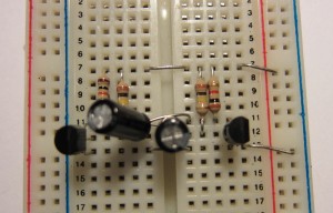
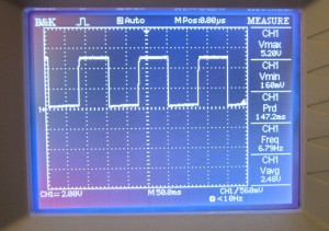
Connecting an oscilloscope to output O2, the result shows a decent square wave with 50% duty cycle at about 6.7Hz. Looks quite nice.
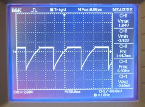 I also checked the signal on T2’s base pin. The result is on the left. As you can see, the beginning of stage 2 is signaled by the jump to a large negative value. During this stage, C1 charges through R2, so T2’s base voltage rises continuously. As soon as it crosses Vb, T2 conducts, and its base remains at Vb until the start of the next cycle.
Next, let’s blink some LEDs with the oscillator. You can either connect LEDs in series with R1 and R4, or directly to output O1 and O2. Check the video below (the circuit below uses C1=C2=10uF):
Finally, if you want, you can make a printed circuit board, so you can carry it around, or use it to decorate a toy with flashing LEDs. Enjoy!
Appendix
Frequency change when connecting LEDs with R1 and R4 in series
As mentioned above, one way to connect LEDs into the multivibrator is by putting them in series with R1 and R4. One interesting thing I noticed is that when doing so the frequency of the LED blinking is much faster than the calculated frequency. So what’s happening? A careful analysis reveals that this is not surprising. The main reason is that because the LED will drop about Vled=2V, C1 and C2 will not be charged all the way to Vcc-Vb anymore. Instead, they are charged to about Vcc-Vb-Vled. Consequently, it takes less time for C1 or C2 to charge from a negative voltage to +Vb, hence the oscillation frequency is faster. The precise formula is actually:
Since Vb+Vled is quite significant compared to Vcc, we cannot make the same approximation as above anymore. For example, with the given values in the first schematic (C1=C2=1uF, R2=R3=100K), and assume Vcc=+5V, the frequency is now roughly 10Hz (compared to 6.5Hz when LEDs are not connected). So this explained why the LED blinking speed seems faster than calculated.
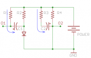 Stage 1
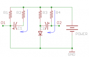 Stage 2