An EagleCAD Script for Creating Laser-Cut Project Enclosures

When designing electronic circuits, often it’s necessary to have a proper enclosure for the project, to protect the circuit board and components, and for aesthetic reasons. There are several options to choose from. For example, if this is a one-off project, you can pick an off-the-shelf enclosure, make custom cutouts to fit the PCB and its buttons, connectors etc. But you will be limited by the enclosures available on the market, and you have to design the PCB size and screw hole locations according to the enclosure, so it’s not very flexible. You can also use 3D printing to make a custom case that fits the PCB nicely, but 3D printing is generally slow, and cheap 3D printers have poor precision. If you are making a commercial product and need volume production, you can order an injection mold, and the injection-molded enclosure fits the circuit perfectly. But you have to spend costs thousands or tens of thousands of dollars to order the mold, and this upfront cost is too much for small-scale projects.

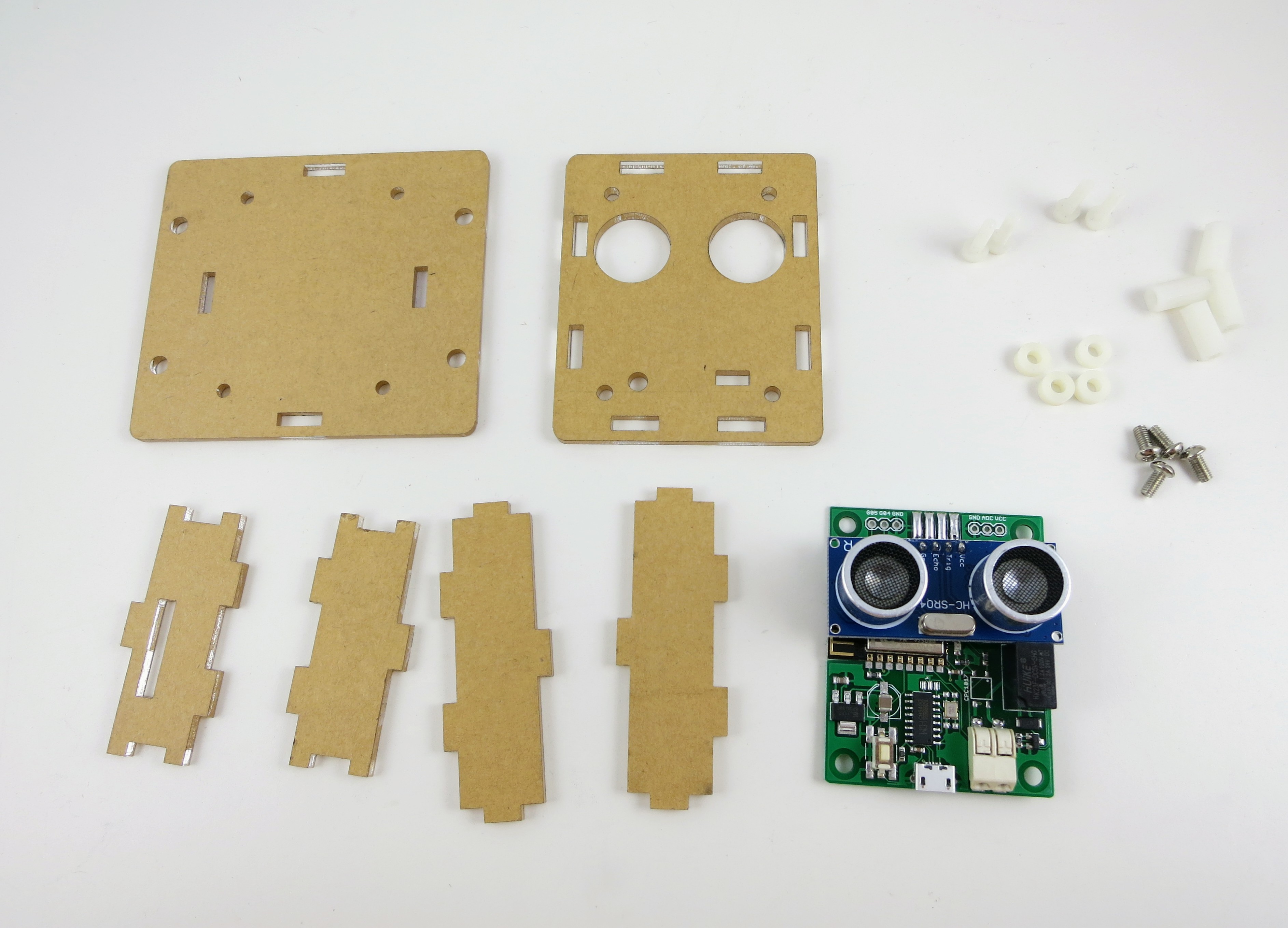
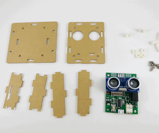
Since last year I’ve been experimenting a lot with laser-cut acrylic enclosures. Compared to the other options, laser-cut enclosures are very easy to customize for the particular PCBs I have designed; they are relatively cheap and fast to make, you can add text engravings to them, and there is no upfront cost. So I have been using laser-cut enclosures a lot for a variety of electronics projects. Generally speaking, the enclosure consists of six pieces of laser-cut acrylic panels, with teeth and holes on the side to lock them together and form a box. You can use plastic or copper screws and pillars to secure the PCB inside the box. As a side benefit of this type of enclosure — if you happen to make a mistake on one panel (which I did a few times), you can just re-order that particular panel so it’s very easy to re-design and correct the mistake.

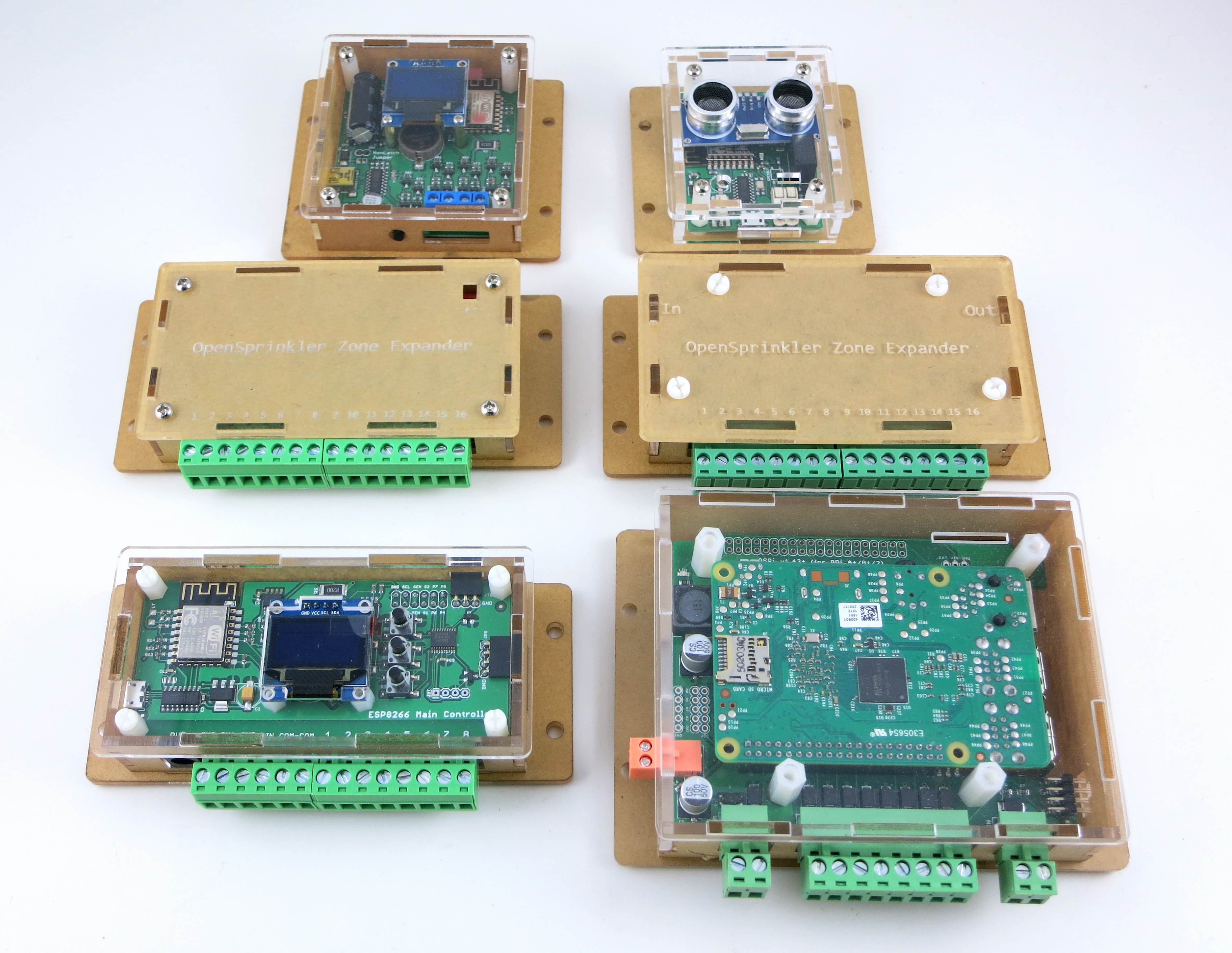
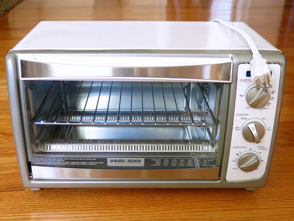
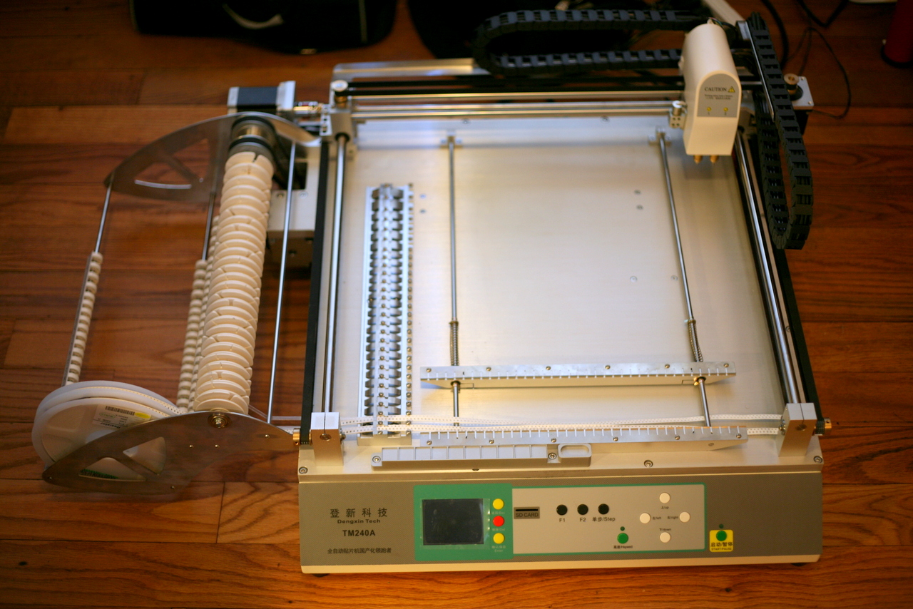
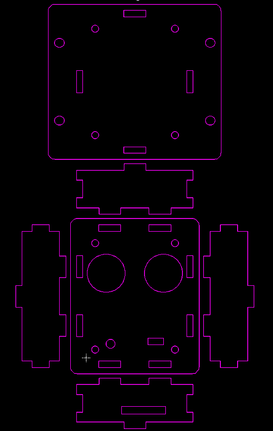
When I started, I found some tutorials and design tools online, to help create the six panels. But they are not really convenient or easy to work with. Because I routinely use EagleCAD to create my circuit boards, it would be really nice to have a enclosure design tool inside EagleCAD, so that I can compare the enclosure with the PCB precisely, making sure that all the cutouts are in the correct locations and have correct sizes. So a little while back, I wrote an EagleCAD script to help me create laser-cut enclosure panels, and used it to create a variety of project enclosures, as shown in the picture below.

Below I will briefly walk through the details of the script, what the various parameters mean, and I made a video to demonstrate how to use this script. To begin with:


Video Tutorial


Explanation of Parameters

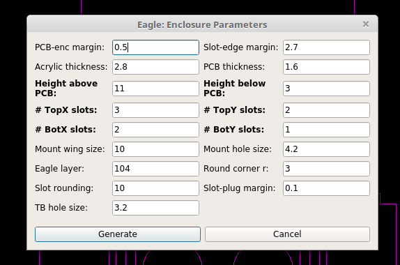
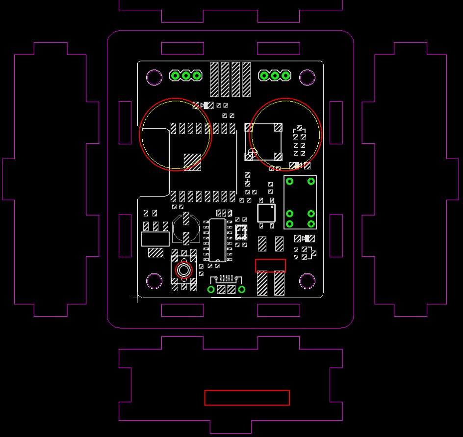
The way this script works is that it follows the dimensions of your PCB outline to create the six panels. It assumes the PCB is rectangular shaped, but if needed you can modify it to support non-rectangular shaped PCBs. There are a number of parameters you need to set, which I will briefly walk through below. Most of them are best explained by the annotated images below. All parameters of lengths are of unit millimeter (mm).

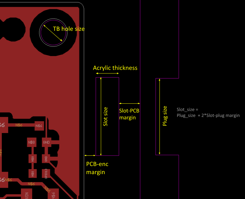
  • PCB-enc margin: the margin from PCB border to enclosure interior border.
  • Slot-edge margin: the margin from the slot boundary to enclosure edge.
  • Acrylic thickness: the common acrylic material I’ve used are either 2mm thick or 3mm thick. You may have to adjust this slightly according to your supplier’s acrylic material thickness. You may want to make this slightly larger (like 2.1mm and 3.1mm respectively) to account for error and variations in the actual material.
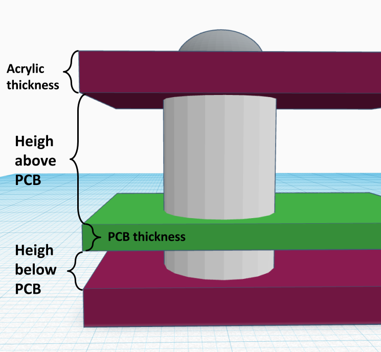
  • PCB thickness: standard PCB thickness is 1.6mm, but there are other choices too, like 1mm, 1.2mm, 2.0mm etc.
  • Height above/below PCB: this defines how much space there is above and below the PCB (NOT including acrylic). The ‘above’ height depends on the tallest component on your PCB. The ones I commonly use are 11mm and 13mm. The ‘below’ height is typically 3mm, to provide spacing underneath the PCB for through-hole components.
  • Top/Bot X/Y slots: define the number of slots on the top/bottom panel and in the x/y directions. The number of slots depend on the length in x or y: longer edges probably need more slots. Also I generally make the number of slots on the top and bottom panels different, to make it easy to identify the orientation of the side panels.
  • Slot rounding: this will round the slot size to the nearest (ceiling) multiple of the slot rounding number. The slot size is automatically computed based on the number of slots. If you want the slot size to be rounded to the nearest multiple of 10, for example, you can set slot rounding to 10.
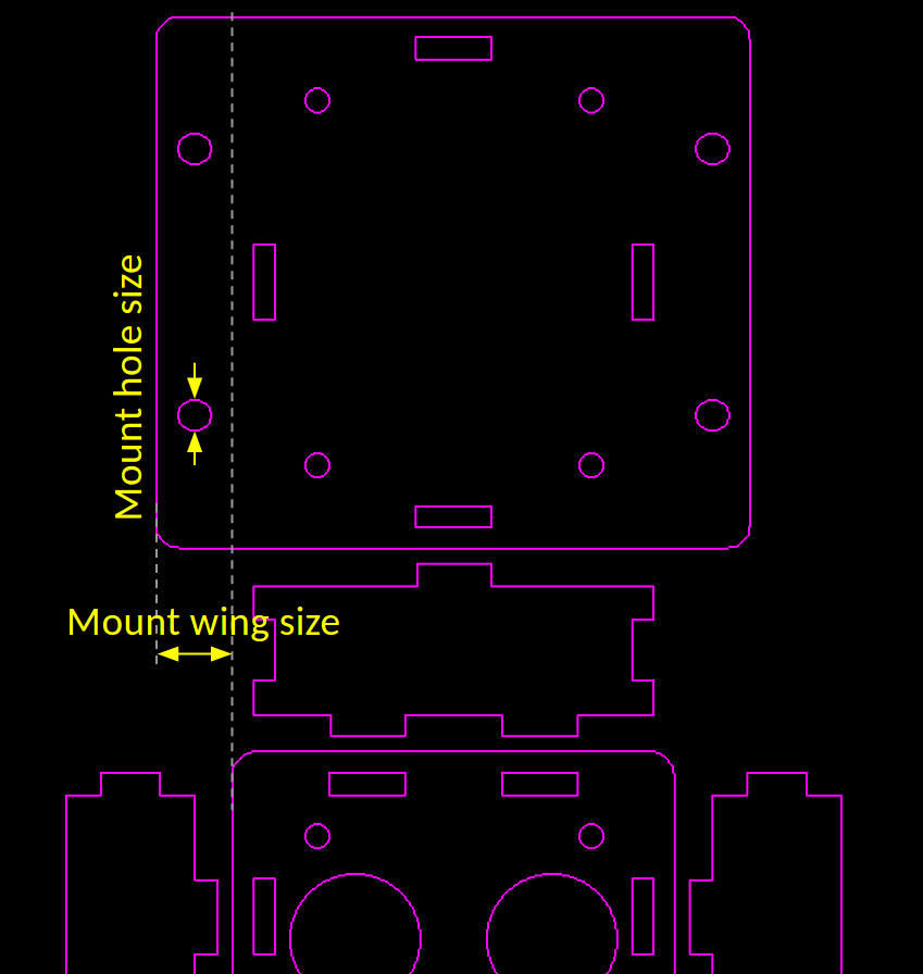
  • Mount wing/hole size: if you need the back panel to be wall-mountable (which is generally the case for my boards),
    you can define the width of the wing and mount hole size (diameter).
  • Round corner r: radius of the rounded corners.
  • Slot-plug margin: this will shrink the plug size slightly to make it easy to insert into the slot. The default is 0.1mm but I suspect leaving it 0 is fine (because laser cut holes generally have negative error, meaning they are larger than design).
  • TB hole size: top-bottom hole size. This is set according to the size of screws/pillars you need. For example, if you plan to use M3 screws, set this to be slightly larger than 3.0; if you plan to use M4 screws, make it slightly larger than 4.0 and so on.
  • Eagle layer: defines which Eagle layer it uses to draw the enclosure. By default it uses layer 104.

Running the Script: upon running the script, it will hide all layers except the Acrylic layer (104 by default). This allows you to see the overall enclosure design. You can go back and un-hide the other layers. If you re-run the script, it will remove the existing content on the Acrylic layer, and re-create the outlines. So be careful re-running the script — if there is anything you want to preserve (such as custom cutouts as explained below), you want to put them in a different layers so that they don’t get wiped out.

Annotated figures are more intuitive for explaining the parameters:

Creating Custom Cutouts and Text Engravings

The script doesn’t automatically create cutouts for connectors, and that part you have to do it yourself. Still, having the enclosure outline embedded with the PCB design makes it easy to align the cutouts with the connectors. As shown in the last image above: the custom cutouts (colored in red) are embedded in the PCB design, so you can precisely align each cutout with its designated connector. I generally create the custom cutouts in a different layer, so that in case the Acrylic layer gets wiped out, the cutout layer is still preserved. You can also add text engravings — where I order acrylic pieces, they can add laser engravings for only a small amount of additional cost. So if I need any labels for the connectors, I can easily add them to the custom cutout layer and get them ordered as engravings.

Order Laser-cut Acrylic Pieces

Once the design is finalized, I place an order from a vendor on Taobao.com — the Chinese equivalent of eBay. To prepare the design for ordering, I export the Acrylic layer and Custom Cutout layer together into a DXF file in EagleCAD, then convert it to Adobe Illustrator (.ai) file, and send it to the vendor. I then specify the acrylic thickness, color (the most common is transparent, but there are a variety of other colors to choose from). Make sure the scale of the design is appropriate — Chinese vendors work with millimeter (Americans should too!), so make sure the design is scaled to the correct millimeter scale, which you can do easily in Illustrator.

Assemble the Enclosure

Assembling the enclosure is fairly straightforward: it involves a set of screws on the top panel and bottom panel, and separation pillars below the PCB and above the PCB. I generally like plastic screws and pillars as they are much lighter than iron or copper screws and pillars. The acrylic pieces come with a brown protective sticky paper cover. You can peel the sticky paper cover. If the acrylic material is transparent, you can see through the enclosure to the circuit board, which looks pretty cool. I generally only peel the top panel and keep the protective cover on the other panels, because peeling a lot of paper is tedious, and the brown paper cover gives a wooden appearance, which is not bad. So I keep them as much as possible. To peel the cover, it’s best to use another acrylic piece, or a stiff card of some sort to lift the cover from one corner, then carefully peel and remove the entire cover. Don’t use your nail as it can easily damage your nail. Acrylic is reasonably scratch-resistant, so using another acrylic to help peel it is totally safe.

The GIF below shows the assembly process:

Limitations and Todo for the Future

Perhaps the biggest limitation of laser-cut enclosure is the assembly time — putting all those screws and pillars together cost time and labor. But given that there is no upfront cost, it’s pretty suitable for small-scale projects, or serving as a temporary enclosure until you have a more permanent solution like an injection mold. In addition, for DIY-style projects, you can give the enclosure pieces to the customers and let them assemble the enclosure. It’s actually quite fun, kind of like the philosophy of Ikea furniture — its value is not only in the low cost but getting yourself involved in assembling the product provides a more engaging experience.

There are a couple of improvements I want to make to the script and I will try to work them out in the future. One is the ability to create a local file to store the parameters. At the moment if you want to re-design the enclosure for the same circuit, you have to manually remember what parameters you have used before — the script doesn’t remember the previous parameters because every time you run it, it will load the default parameters. It would be nice for it to store previous parameters for a particular circuit board to a local file, making it easy to modify in the future. Another improvement is providing visual aid to indicate where the PCB is located on the side panels, to make it easier to design cutouts for connectors etc. Right now to create cutouts I still have to do a lot of hand calculations, which can be automated in the future.

That’s it. Feel free to try it out and let me know what you think. If you make modifications to the script and improve its features, please be generous to share your contributions!

Review of NeoDen 4 Pick and Place Machine with Vision System

A few years ago I purchased a NeoDen TM-240A desktop pick and place machine, and wrote two blog posts about it. It was one of the most popular desktop pick and place machines on the market back then, and has served me well for the past three years. It does small boards pretty well, but without a computer vision system, it requires a fair amount of manual placement of fine-pitched components; and it only has a fixed set of 27 feeders, which are not entirely sufficient for me.

Recently NeoDen released a new model called NeoDen 4 — it’s their first desktop model that has built-in computer vision system. The vision-based alignment makes it possible to place fine-pitched components with minimal manual work. It has four pick and place heads, which means if can simultaneously pick up to four components at a time. It can fit a lot more feeders, and can handle a variety of component types, including matrix tray components, and any special components that you can lay out in a 3D printed tray. It has a vibration feeder for components in tube packaging. Although I rarely use tube packaging, one notable exception is the CH340G USB-serial chip, which is used in almost all my products, and so far it only comes in tubes. On top of these exciting new features, the machine I ordered comes with a PCB conveyor belt that can automatically feed PCBs into the system. This is really convenient for starting a pick and place job.

img_20160916_162204img_094454

Well, a picture is worth a thousand words, and a video is worth a thousand pictures! Without further ado, here is my video review of this machine:

So far I am pretty happy with the machine. Pricing-wise, it’s surely more expensive than TM-240A, but not significantly. I paid around 9K in total, including DHL shipping and all the feeders (for TM-240A I paid 5.5K). It’s not all perfect so you’ve got to learn the quirks. For example, I learned that the component height is often quite important — without providing the proper component height, the placing may give you a lot of troubles. Also, for components that need better placement accuracy, reducing the placing speed (say, to 50%) helps a lot to improve the accuracy and reliability.

Overall the machine operation is fairly intuitive, and it works in a predictable manner, much better than some of the comparable products I’ve seen on the market. No matter how powerful the machine is, you can’t afford to spend forever learning how to use it. It took me just two days of looking through the user manual, video tutorials, and doing my own trial and error to learn to successfully produce the first board using this machine. I would say it’s pretty good.

Disclaimer
I am not associated with NeoDen in any way. I am just a standard user. Please do NOT contact me for purchasing or sales questions. Go to their company website (www.neodentech.com) for details.


EagleCAD ULP Script

One difficulty I had initially was how to export a PCB design to a format acceptable by the machine. Without this I would have to manually locate the x-y coordinates of each component using the down-facing camera, which would be a huge pain. The user manual and video tutorial had no descriptions about the format of the spreadsheet. After banging my head on the wall for a while, I found one example spreadsheet somewhere in the flash drive that came with the machine, and that seems to work. Then I went ahead and modified an existing EagleCAD script (designed for TM-240A) to match the example spreadsheet. The script can be downloaded from the link below. Please take a look at the README file as it explains how to use the script.


A Pleasant Visit to Worthington Assembly Inc.

I had an amazing day visiting Worthington Assembly Inc. (WAi) — an electronics manufacturer / circuit assembly company located in South Deerfield, MA. It’s only 15 minutes of driving from Amherst, where I live. I first saw their business name when I was reading Ryan O’Hara’s post about how he got his RGB-123 LED matrices manufactured. I must have had a lousy day then, because I failed to notice the location of the company, and had always thought it’s in Boston. Then last night when Andrew Seddon, CEO of CircuitHub.com, pinged me about PCB manufacturing and mentioned WAi, I suddenly came to realize that they are located right next to me. Gosh, I felt completely dumb that I didn’t find this out earlier!

Anyways, I couldn’t bear with the temptation to check out their facilities, so I paid a visit right away this morning. It really made my day — the beautiful pick and place machines, conveyor belt reflow oven, selective soldering machine, it’s like a dream circuit assembly house I’ve always wanted. Chris Denney (CTO) gave me a tour around the house. I was too engaged in the conversations and didn’t take as many pictures as I wanted. But here are a few:

wai_visit003wai_visit001
On the left, Quad QSP-2 picker that’s being retired (at the end of the picture is their Vitronics Soltec reflow machine); on the right: through-hole component insertion machine.

wai_visit005wai_visit004
MyData picker that’s currently in service. This one can pick 8 components at a time, and has a super fast vision system that does alignment in real time. It also has a mechanical alignment system, and a component checking system that can read component values (e.g. resistance, capacitance) on the fly. Amazing!

wai_visit000wai_visit006

Selective soldering machine, and PCB cutter.

Very satisfying. I can even imagine the next batch of OpenSprinkler to be assembled right here. Then I can just drive up in 15 minutes to pick up the order. How cool is that 🙂 They take both large-quantity and small-quantity orders, down to even just 1 board, surprisingly. Of course the cost of making just 1 board would be quite high, compared to making 100, where the same overhead cost will be amortized.

Right now they are in partnership with CircuitHub.com to make the service available to makers and hardware startups. If you have circuit assembly need and don’t have the resources to make them yourself, or if you have the resources to make a few but not hundreds, you should definitely give it a try. Just log in to CircuitHub.com (with your dropbox account) and upload some Eagle project files. The user interface is very clean and friendly. It links to Octopart.com to grab component prices in real-time. You can then adjust the order quantity and lead time. Kudos to Andrew for building such a slick website.

I was very well treated, had Polish beer with Neil, Rafal, and Chris; and by the end of the day, I even got two free T-Shirts. Cool. Picture moment!
IMG_0036IMG_0037

Reflow Toaster Oven with Bells and Whistles

A reflow oven comes in handy when you work regularly with SMT circuits. I’ve had the T-962A reflow oven for about a year now. While it has worked reasonably well, recently it has started showing some signs of aging. First of all, the total reflow time is quite long, about 15-16 minutes. This is really slow. Worse even, occasionally the internal temperature sensor would have a hiccup and the boards would come out under-heated or over-heated. Also, I hate the built-in buzzer, which produces a very loud, high-pitched beep when reflow is completed. This is very annoying — since I keep the reflow oven outdoors, I didn’t want my neighbors to think the beep is my fire alarm. So it’s time to find an alternative / backup solution.

After some online research, I’ve decided to build a reflow toaster oven using an Arduino-based controller. Toaster oven is cheap and provides better, more even heating than a hot skillet. I know toaster oven reflowing has been blogged about everywhere, but I do want to give my version some bells and whistles to provide more convenience. For example, I typically keep the reflow oven outdoors on my porch while working in the basement. So I’d like to receive a remote notification when reflow is complete (no loud beep please!). Also, I’d like an automatic way to open the oven door and blow air into the oven to accelerate the cooling time. For remote notification, I’ve decided to use an 433MHz RF transmitter to send signals to a remote power socket. I have a lamp connected to the power socket, and this way I will get notified when reflow is done. For faster cool-down time, I will use a servo tied to the oven door handle with a string — rotating the servo shaft can pull the door open. I will also put a second remote power socket connected to a circulation fan to blow air into the oven. Since I am using remote power sockets anyways, I am going to throw in a third one for the oven. This way all power line devices are controlled by power sockets, so there is no messing around with cutting cables etc. If you want better reliability, you can certainly use a relay or an SSR. I just decided to go with RF power sockets for the convenience.


Materials
Here is the list of materials I used:

IMG_3591IMG_3593IMG_3594IMG_3595
I have an existing set of RF power sockets and I don’t remember where I got them. But the link provided above looks similar, so they should work fine. A quick note: there are cheaper RF power sockets which only support toggling, but I would suggest getting the type that has separate on/off buttons for each channel, because you can know for sure whether the socket is on or off. Also, there are some types which work in the 315MHz frequency band. In this case, you need to get 315MHz RF transmitter instead of 433MHz.


Step 1. Temperature Probe
The reflow oven is a temperature-controlled device, so the first thing to do is to have the microcontroller sense temperature. The cheap kitchen thermometer is perfect for this: it has a thermistor (i.e. temperature-sensitive resistor) wrapped around a metal probe. Just open the thermometer, desolder the two wires, and extend the wire length by soldering two pieces of longer wires. I also used some hot glue to fix the joints so they they won’t move around and break.

IMG_3597IMG_3598IMG_3607IMG_3596

Next, measure the diameter of the temperature probe (mine is about 0.147″), and at the back of the toaster oven drill a hole that’s slightly bigger (I used 5/32 drill) than the probe size. The hole should be located at roughly a quarter to one-third on the height, so that when the probe is plugged in it would neither touch the top heating element nor the tray. Next, wrap a layer of Kapton tape around the temperature probe, and insert it through the hole, so that it stays tight in place.

The oven should be set to the highest temperature, convection, and stay on. This way we can bypass the oven’s internal control mechanism and instead use the microcontroller to turn heating on and off.
IMG_3599IMG_3602IMG_3603IMG_3606

For the microcontroller to sense temperature, just use the 2.32K resistor to form a voltage divider with the thermistor (i.e. probe). See the schematic on the right below. The divided voltage is connected to Arduino’s analog pin A0 for reading.

IMG_3608t_volt_divider


Step 2. Temperature Calibration
The next step is to perform temperature calibration. If you’ve got the same kitchen thermometer and 2.32K resistor as I have, you can skip this step. But if you have a different set, you need to perform a calibration step to find out the relationship between the actual temperature with the analog reading. To do so, I used an existing digital thermometer (my EX330 multimeter) to serve as reference. Insert its temperature probe to the oven and get the tip close to the center; then I wrote a simple Arduino program to print out analog values from A0 once every second. Turn on the oven to let it heat up. The temperature will rise, and the analog reading also rises.
IMG_3609IMG_3610IMG_3611

When it reaches about 210°C (Celsius), turn off the oven, and record the analog reading. Then do another reading when the temperature drops to about 170°C, and the last one when it drops to about 80°C. Basically 210°C is when we should stop heating (the temperature will climb up a little more beyond 210), 170°C is when the oven door will open and the fan will kick in, and 80°C is when the reflow is considered finished. My readings corresponding to these three temperature values are roughly 830, 790, and 360. These will be used in the Arduino program later.

IMG_3612IMG_3613IMG_3614


Step 3. Oven Door Opener
Next is a fun step. I built a oven door opener using a servo. The basic idea is to attach a piece of string between the servo and the oven door handle. Rotating the servo shaft will be able to pull the door open. To do so, I picked up some pieces of wood from HomeDepot and build a wooden frame. To make the whole assembly stable, the base of the frame should be sufficiently heavy. Then I secured the servo to the frame using some long #4 screws and nuts. Since the servo doesn’t come with a long shaft, I used a small piece of wood and attached it to the servo gear. This can extend the sweeping distance of the servo. Be careful not to make it too long though, otherwise you may overdrive the servo’s torque.
IMG_3620IMG_3621

The video below shows the servo in action. This is using Arduino’s built-in Servo example called Sweep. The servo’s three pins are connected to 5V, pin D9, and ground.


Step 4. Remote Power Sockets
The next step is to interface with the remote power sockets. I’ve written a previous blog post about this. Since then I have discovered the RC-Switch Arduino library. This is a very useful library that can automatically decode the signal patterns from most common remote power sockets. All that’s required is an Arduino and a RF receiver. I wired up my 433MHz receiver to the Arduino, and used the library’s receiver example to figure out the following binary code for my power sockets:

  • Channel 1 on: 010101010011000101000011; off: 010101010011000101000000.
  • Channel 2 on: 010101011100000101001100; off: 010101011100000101000000.
  • Channel 3 on: 010101010000110101110000; off: 010101010000110101000000.

Once the patterns are figured out, I can then connect a 433MHz transmitter to Arduino to simulate the remote control. This way I can reliably turn on and off each socket individually.


Step 5. Putting Everything Together and Testing
Now all the ingredients are ready, it’s time to put everything together for testing. The Arduino pin assignments are: temperature probe on analog pin A0, servo on digital D9, and RF transmitter on D10. The power sockets assignments are: toaster oven on channel 1, fan on channel 2, and lamp on channel 3. Since the controller will be used outdoors on the porch, I found an enclosure that can fit everything nicely inside. I also soldered a wire to the RF transmitter as an antenna to extend the transmission range. The power comes from an external 5V adapter. Please check the video at the beginning of the post for demonstration. The controller program source code can be downloaded here:

IMG_3622IMG_3623

With the capability of opening oven doors and blow air into it, the cool-down time is significantly faster. The total reflow time is about 6 minutes now, which is a lot better than 15 minutes before. That’s it, my reflow toaster oven with bells and whistles. It can certainly be improved by adding PID control, The hardware cost, everything included, is about $120. It’s inexpensive and pretty easy to replicate. Much better than my professional reflow oven!


First Try on Panelized PCBs

As I am getting more experienced with the TM-240A pick and place machine (in the following I will call it the PNP machine, as in PNP transistors 🙂 ), I’ve been thinking of ways to improve productivity. One obvious way is to panelize PCBs, meaning to assemble multiple copies of the PCB onto the same board. This can help greatly reduce the overhead time of stenciling and PNP loading time. I have to admit, I’ve never done PCB panelization before. I did search online and found various tutorials, but it’s unclear to me how to exactly indicate the ‘V-cut’ layer to the PCB manufacturer.

But I found an easier route. Recently I’ve been ordering PCBs directly from a Chinese company called 深圳嘉立创 (http://www.sz-jlc.com). I got to know this company very randomly, actually through watching the beginning clip of the SparkCore Kickstarter video. The company has a very streamlined PCB manufacturing process, where you can track each step of the PCB making, all the way from drilling, to printing layers, to etching, to optical inspection, to solder-mask and silkscreen printing, to testing, and to shipping. It’s completely amazing (except the website only has Chinese version…). Anyways, when you order PCBs from their website, apparently you can specify how you’d like to panelize your PCBs. You don’t need to panelize the PCB yourself in Eagle (which I haven’t learned how to do yet), but you just need to describe your panel design (like 2×3, 4×4 etc.), and they will do the panelization free of charge. Isn’t that awesome?

Since this is the first time I’m ordering panelized PCBs, I wanted to be careful. So I ordered a very simple board — the OpenSprinkler Zone Expansion board, with the simplest panelization — 1×2. And the image on the left below shows what I received. Very neat. I also asked them to add an extra 10mm border on each side, and fiducial points (these I paid extra for). Since the board is not rectangular shaped, the panel comes with routed edges on the curved sections, and V-cuts on the straight lines. This way, it can be easily de-panelized by simply snapping each board off along the straight edges. Pretty awesome, especially considering I didn’t have to do anything in Eagle to create the panel design 🙂

IMG_0066IMG_0065

So what’s the picture on the right above? This is also something new to me: apparently when you order PCBs from the company, you can also order a laser-cut solder paste stencil to go with your PCB order. It’s only 10 extra bucks, almost a no-brainer. I ordered one for this particular batch, so I can experiment with it. The stencil is made from a steel sheet, and mounted on a metal frame. It’s quite large (37cm x 47cm), so you will need a stencil printing machine that can handle a board of this size. Fortunately I got a fairly big manual stencil printing machine a while back, so I can put it to good use now.

IMG_0067IMG_0069

In order to use the stencil, the first thing I did was to mount the stencil frame onto the printing machine. Once mounted, you can easily lift the stencil up and down, to quickly insert and take out stenciled PCBs. Then I aligned the PCB to the stencil holes. This is very tedious — since the stencil is made of steel, which is opaque, there is no easy way to align them. I had to do a lot of trial and error and eventually was able to get them perfectly aligned. Once aligned, temporarily fix the PCB in place by using some tape. Finally, use three old PCBs to make a frame around the center PCB. Then you are all set.

With the stencil printing machine (albeit manual), applying solder paste works like a charm, and is much faster than using my home-made stencils. The stenciling quality is also excellent (see the picture on the right below). Apparently they optimized the stencil design, and created small ‘crosses’ around relatively big (0805 or above) components. This prevents the solder paste from smearing underneath the stencil. Very smart!

IMG_0072IMG_0079

Next step is to populate components. The TM-240A pick and place machine supports PCB panelization. All that I had to do was to open the existing PCB configuration file, and add a new line for each additional sub-board, indicating the amount of shifting from the first sub-board. With this simple change, the PNP machine can now populate twice as many components, a real time-saver!

IMG_0074IMG_0076

Here are pictures of four boards before and after reflowing. The reflowing quality is pretty good.

IMG_0077IMG_0081

Finally, to separate the boards into individual pieces, as I said, just snap the boards along the V-cuts. Use some strength along the cuts, and they should come off pretty easily. Here are the final results (with the through-hole pin headers and screw terminals soldered in place). Neat, isn’t it 🙂

IMG_0082

So, to summarize, it takes very minimal effort to make panelized PCBs. First, when ordering PCBs, tell the manufacturer how you would like to panelize the board. They will do the work for you. Next, order a professionally made solder paste stencil with the PCB order. Finally, modify the pick and place configuration file to reflect the number of sub-boards and the shift amount of each. That’s it. Not bad at all!

NeoDen TM-240A Automatic Pick and Place Machine Demo — Part 2

Updates

  • Click here to see NeoDen 4 Pick and Place Machine with Vision System.

This is Part 2 of the NeoDen TM-240A pick and place machine demo. Today I placed the machine on a proper table downstairs in the basement, and had my first-hand results of a production run — namely using the pick and place machine to assemble the OpenSprinkler Pi circuit board. The results are pretty satisfactory. Here is a video demo:

Now I will explain the boring details 🙂 The first step is to load the component tapes. The user manual has no instructions on how to load the tapes, so you have to carefully watch the videos provided by the manufacturer to learn. OpenSprinkler Pi is relatively simple so it doesn’t require many components. The TM-240A can fit twenty-one 8mm tapes, four 12mm tapes, and two 16mm tapes. While this is almost twice as much as its sister model TM-220A, the 12mm and 16mm slots turn out to be quite precious — those can easily run out and you will have to place the remaining components by hand. In my case, I also have a few relatively bulky components (e.g. LM2596S in TO263 package, and surface mount inductors and battery holders) that I have to place manually. So these components will all be hand placed after the machine pass.

On TM-240A, there is a front component loader that can fit 10 ad-hoc components. These can be bulky components that are not handled by the standard feeders. This is a very nice feature, however, the downside is that for each slot only allows one component, so you will have to re-load for each circuit board.

Next, I made a configuration file for the PCB. I started by using the Eagle script file downloaded from this link. I appreciate the author for sharing the script, as it saved me a lot of time of trying to figure things out myself. The configuration file is a human-readable text file and is very easy to edit. For example, for any components that I want to place manually, I simply put a value of ‘1’ in its ‘Skip’ column. Also, you can manually refine the x-y placement of each component based on the outcome of a trial run. You will probably have to sacrifice some components while tweaking the configuration file. To avoid wasting solder paste, I used the double sided tape that came with the machine, which allowed me to do trial runs as many times as I want. Once the configuration file is finalized, you can then switch to stencil printed PCBs.

Next, I applied solder paste to the PCB using my home-made solder paste stencil. I then placed the circuit board on the PCB holder of the machine. Make sure you push the PCB all the way to the left. Because my PCB is not perfectly rectangular, the machine’s origin is not aligned with the PCB’s origin. To fix it, I simply write down the amount of origin shift in the configuration file. The shift amount can be either calculated from the board design file, or can be measured empirically.

The exciting moment starts after clicking on the machine’s ‘Start’ button. It’s quite pleasing to see the machine moving quickly and precisely, picking up components and dropping them down on the circuit board. The machine can automatically detect if a component has been picked successfully (based on its internal pressure sensor reading), and make up to three attempts if it fails. The machine is also equipped with two needle heads. I installed a smaller needle, suitable for 0603 and 0805 components, as well as a bigger needle, suitable for components on the 12mm and 16mm tapes. The dual-head design is very convenient, as I basically never have to change the needles any more.

With less than 20 components to place, the machine finishes each pass very quickly. From the video you can see that a few components are not aligned perfectly, but these present no problems at all for the reflow process. Indeed after reflowing, most components will get aligned well with the solider pads. Well, to be fair, I’ve used mostly large components (e.g. 0805), and have yet to try smaller components. So I can’t say if the accuracy is sufficient for boards mostly populated with 0402 components. But I am pretty sure 0603 should be all right.

Anyways, I hope the video has given you some ideas of the capabilities and limitations of this machine. The next steps I would like to try include adjusting the speed of the machine to see if that helps with the placement accuracy, paneling the PCB to improve productivity, and also try to use the front loader for some of the bulky components. Feel free to leave your questions and comments below. Thanks!

New Toy: NeoDen TM-240A Automatic Pick and Place Machine – Part 1

Updates

  • Click here to see NeoDen 4 Pick and Place Machine with Vision System.
  • Click here to see Part 2 of the TM-240A video.

Yes, there have been lots of new updates recently. Among them is a new toy I received in the mail today: a NeoDen TM-240A automatic desktop pick and place machine! I’ve kept my eyes on this baby for a quite a while, and finally decided to make a purchase last week. The shipping was very fast: DHL from China, a total of 4 days from shipping to delivery. The package is quite heavy: 65kg with the box, and 45kg just the machine itself. The DHL courier and I moved it together to my workshop. Some unboxing pictures:

IMG_2664IMG_2668IMG_2671IMG_2672

So what’s a pick and place machine? Simply speaking, it’s a machine that can quickly and accurately place SMT components onto a PCB. As our orders keep increasing, we need better tools to significantly improve the manufacturing productivity. It’s true that the major manufacturing needs can be outsourced to companies like SeeedStudio, but you will always have to prepare for unexpected delays. Also, small production runs are not worth outsourcing to China. So it’s crucial to have in-house manufacturing capability to meet small production needs.

The basic tools for small-scale PCB assembly include a stencil printing machine, a pick and place machine, and a reflow oven. The pick and place machine is probably the most expensive among the three. The NeoDen TM-240A is a relatively low-cost model. It’s desktop-size, so it’s light-weight and doesn’t take a huge amount of space. It has built-in suction pump, 28 feeders, two placement heads, speed of 7000 components per hour, and a maximum PCB area of 400mm x 360mm. It costs about $5000, which is significantly cheaper than machines at similar specs. I’ve seen machines that cost at least 10K, and even at that price you have to buy feeders separately. There is a sister model to TM-240A, which is TM-220A. It’s cheaper (~$3600), but with less feeders and smaller PCB area. The downside of TM-240A is that it does not have a vision-based system, so it’s not as accurate as the more expensive machines. But considering its price and capability, I decided it’s a good investment.

IMG_2675IMG_2674

I bought the machine directly from the Chinese website Taobao, which is the equivalent eBay in China. Shipping is 3000RMB (~$490). Considering it took only 4 days from China to the US, it’s not a bad price. All together I paid about $5500, including the machine and shipping cost.

As soon as I got the machine, I couldn’t wait to open it and give it a try. The user manuals are pretty minimal, but there is an SD card that contains several tutorial videos which are very helpful. For example, the user manual does not explain how to install the component tapes, and it took some careful watching and rewinding of the tutorial video to figure it out. The package came with a sample PCB and a bunch of double-sided tape. Using these I could quickly set up a test run without applying solder paste at all. The video below shows a demonstration. It’s very exciting to see the machine in action! It’s also quite fast. I am looking forward to using this machine in real production. I am glad that this machine has sufficient number of feeders to handle OpenSprinkler in one pass (i.e. no need to change tapes in the middle). There will be quite a bit of learning involved, but I am hopeful 🙂

Update: Click here to see Part 2 of the video.